
Wafer Back Grinding Process manufacturer Grasping strong production capability, advanced research strength and excellent service, Shanghai Wafer Back Grinding Process supplier create the value and bring values to all of customers.
Wafer Back Grinding Tapes AI Technology, Inc. Wafer Back Grinding Tapes Rework Process White Papers Wafers requiring grinding and .
GDSI, Grinding and Dicing Services complete resource for Silicon Wafers Processing includes Probing, Bumping, Grinding, Polishing in San Jose, California.
Warping of silicon wafers subjected to back-grinding process. This study investigates warping of silicon wafers in ultra-precision grinding-based back-thinning process.
UV Tape is adhesive tape for semiconductor process. ... tape holds wafer strongly in wafer grinding process or wafer dicing process. On the other hand, ...
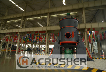
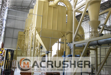
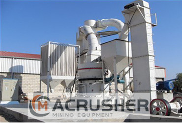
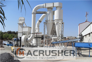
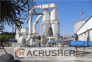
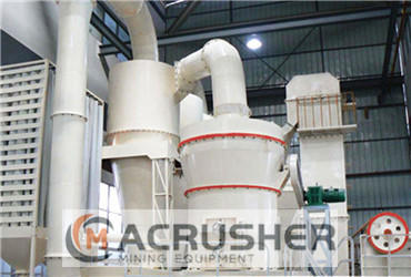
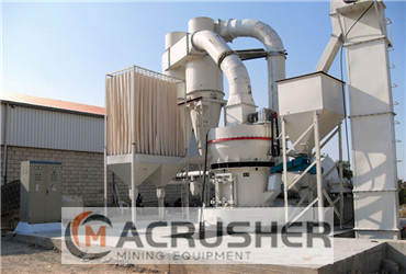
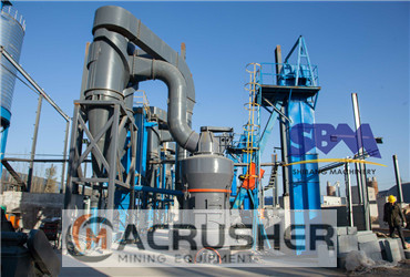
back grinding process + crushergrinder. Wafer backgrinding + Wikipedia, the free encyclopedia Wafer backgrinding is a semiconductor device fabrication step during ...
Wafer Backgrind is the process of grinding the backside of the wafer to the correct wafer thickness prior to assembly. It is also referred to as 'wafer ...
The present invention relates to a process for the back-surface grinding of wafers using films which have a support layer, which is known per se, and an adhesion ...
Effect of Wafer Back Grinding on the Mechanical Behavior of Multilayered Low-k for 3D-Stack Packaging ... generated during wafer back grinding process affect the
Numerical Simulations of a Back Grinding Process for Silicon. Publication » Numerical Simulations of a Back Grinding Process for Silicon Wafers.
Semiconductor Wafer Edge Analysis/4 Stricter requirements in the wafer manufacturing process have made edge measurements important for both 200 mm and 300 mm wafers.
Dicing & Grinding, Greases, Gels & Wax Coatings. Wafer Dicing Tapes; ... Wafer Back Grinding Tapes. ... Consistent bond strength during grinding process;
Silicon Wafer Back Grinding Wheel - Features Thoroughly-monitored manufacturing process for near-zero scratch - Manufactured in clean room class: 100 ~1000
Back grinding is a process that removes silicon from the back surface of a wafer. Silicon Valley Microelectronics provides grinding on our own substrates or on ...
Effect of Wafer Back Grinding on the Mechanical Behavior of Multilayered Low-k for 3D-Stack Packaging ... generated during wafer back grinding process affect the.
A wafer sawing/grinding process capable of removing cracks and chipping resulted from a wafer sawing operation. A silicon wafer having an active surface and a back ...
Effects of back grinding process on ... read more; Wafer dicing,Wikipedia, ... The process of wafer back-grinding induces stress that can propagate into the bulk of ...
Plasma systems for wafer stress relief ... process containing no free ions or electrons that could potentially charge the surface of the wafer. The back-grinding ...
Semiconductor Back-Grinding The silicon wafer on which the active elements are created is a thin circular disc, typically 150mm or 200mm in diameter.
Wafer backgrinding is a semiconductor device fabrication step during which wafer thickness is reduced to allow stacking and high-density packaging of integrated ...
Back Grinding For Bare & Device Patterned Wafers,SVM,Inc. Back grinding is a process that removes silicon from the back surface of a ... wafer back grinding process.
Syagrus Systems thin wafer backgrinding and silicon wafer thinning services meets ... more about our Wafer Dicing Process. ... your next back grinding wafer ...
This study investigates warping of silicon wafers in ultra-precision grinding-based back-thinning process. By analyzing the interactions between the wafer and t
Effects of back grinding process ... Wafer Reclaim and processing services including wafer grinding and thinning, wafer edge trimming, wafer dicing, ...
parallelism between the front and the back surface. Secondly, the grinding ... achieve this we need to understand thoroughly the process of semiconductor wafer grinding